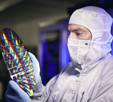
고해상도 이미지 품질의 고객 별 이미징 솔루션
Jenoptik은 귀사를 위한 특정 이미징 개념을 개발하는 전체 서비스 제공업체입니다 - 초기 개념에서 완성품까지.

당사의 고성능 카메라, 이미지 처리 제품 및 완벽한 OEM 시스템은 과학 및 산업 이미징 시장에서 사용하기에 매우 적합합니다: 당사는 개별 프로젝트 및 대량 프로젝트용 모두를 위한 이미징 모듈을 공급합니다.
센서 및 센서 보드에서부터 고객별 응용 분야에 맞는 자체 펌웨어가 있는 카메라 시스템 솔루션에 이르기까지 모든 제품은 전체 가치 사슬을 갖추고 고객의 요구 사항에 정확하게 맞춤됩니다.
고객의 필요에 맞는 소형 CMOS USB 카메라 모듈의 기본 버전을 최적화합니다. 5 메가 픽셀 해상도와 USB 2.0 인터페이스를 갖춘, 이 모듈은 이상적인 플랫폼을 제공합니다. 최단 시간 내에 고객별 수정 사항을 제공할 수 있습니다. 또한 고객의 이미지 처리 응용 분야를 위해하드웨어와 소프트웨어를 약간 변경하거나 다른 모듈에서 전체 시스템을 구축할 수 있습니다.
더 복합적인 프로젝트를 위해, 고객의 요구 사항에 따라 당사의 카메라 모듈의 속성 및 기능을 결합할 수 있습니다.
이런 제품은 다음과 같습니다:
또한 전문 공급망 관리를 제공하므로써 고객을 지원하고, 고객을 위한 전체 가치 사슬을 관리합니다. 고객이 시장에 제품을 신속하게 출시하는 것을 보장하도록 전체 과정에 대한 명확한 개요를 유지하고, 지속적인 성공을 보장하도록 도와드립니다.
센서 및 센서 보드에서부터 고객별 응용 분야에 맞는 자체 펌웨어가 있는 카메라 시스템 솔루션에 이르기까지 모든 제품은 전체 가치 사슬을 갖추고 고객의 요구 사항에 정확하게 맞춤됩니다.
고객의 필요에 맞는 소형 CMOS USB 카메라 모듈의 기본 버전을 최적화합니다. 5 메가 픽셀 해상도와 USB 2.0 인터페이스를 갖춘, 이 모듈은 이상적인 플랫폼을 제공합니다. 최단 시간 내에 고객별 수정 사항을 제공할 수 있습니다. 또한 고객의 이미지 처리 응용 분야를 위해하드웨어와 소프트웨어를 약간 변경하거나 다른 모듈에서 전체 시스템을 구축할 수 있습니다.
더 복합적인 프로젝트를 위해, 고객의 요구 사항에 따라 당사의 카메라 모듈의 속성 및 기능을 결합할 수 있습니다.
이런 제품은 다음과 같습니다:
- 형태인자.
- 해상도 (1 MP, 3 MP, 5 MP, 10 MP, 14 MP, ...).
- 센서 타입 (CCD / CMOS).
- 디지털 인터페이스 (USB 2.0, USB 3.0).
- 광학 인터페이스 (C-탑재, S-탑재, CS-탑재).
- 광학, 필터 및 기타.
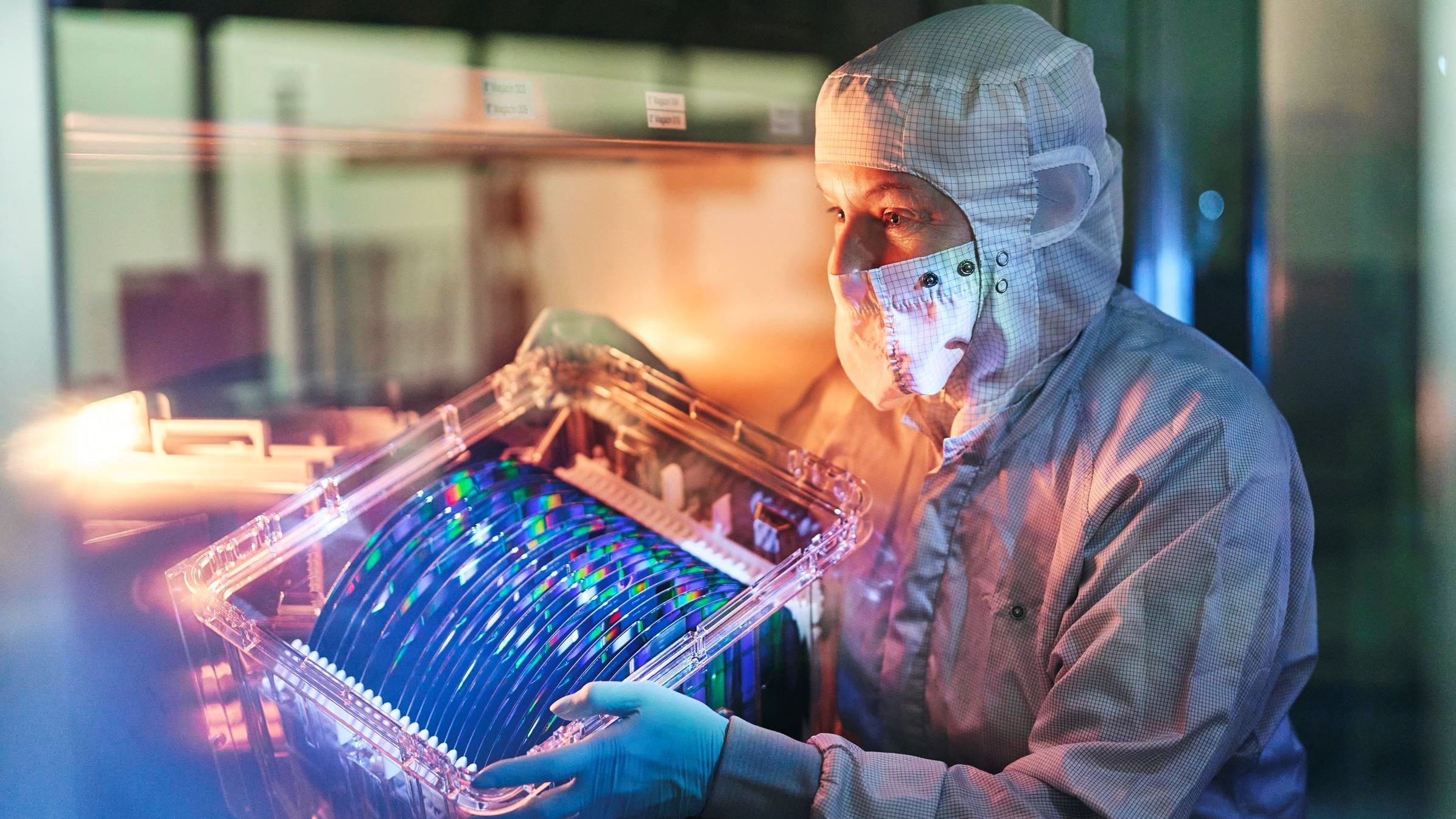
성공적인 이미징 시스템을 위한 전문성
당사는 고객의 성공을 도울 수 있도록 이미징 시스템을 제공합니다. 프로젝트 전반에 걸쳐, Jenoptik 전문가들이 고객을 지원하고 시스템 파트너로서 함께 협력합니다: 설계 과정을 관리하고, 타당성 연구를 수행할 뿐만 아니라 OEM 카메라 설계를 고안합니다. 이를 통해 프로토 타입을 제작할 수 있고 가능한 한 최단 시간 내에 귀하의 이미징 솔루션을 제공할 수 있습니다.또한 전문 공급망 관리를 제공하므로써 고객을 지원하고, 고객을 위한 전체 가치 사슬을 관리합니다. 고객이 시장에 제품을 신속하게 출시하는 것을 보장하도록 전체 과정에 대한 명확한 개요를 유지하고, 지속적인 성공을 보장하도록 도와드립니다.
Our Expertise
- 17 years of know-how in the production of opto-electronic systems
- Unique selling point: Inline LED module measurement technology
- Rapid Protoyping
- Design for Manufacturing
- Well-founded advice on product development, qualification and series transition
ISO Certificates
- DIN EN ISO 9001 (QM-System)
- DIN EN ISO 13485 (Medical Application)
- ISO 14001 (Environment Management System)
Department Production Information
- Department exists since 2006 at Jenoptik
- Area: approx. 400m²
Area consists of two clean room classes:
- 2/3 of the area ISO class 5 (max. 832 particles with 1 µm/m³)
- 1/3 of the surface ISO class 7 (max. 83,200 particles with 1 µm/m³)
Process steps in detail
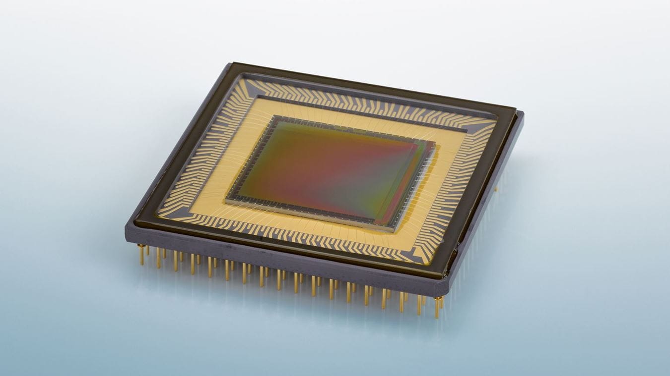
An Imagesensor as example
Learn more about our core competencies for customer imaging modules
Dicing
Die-Bonding
Wire-Bonding
Housing
Testing
Separation
Core competence Dicing

Semiconductor Wafer
Substrate sizes
- Diameter up to 12 inches
- Thickness 0.1mm to 5mm
- Accuracy: up to 2 µm
Creation of negative 3D structures
- Increase adhesive surface for later bonding
- Change reflection characteristics
Full underwater separation option with following benefits
- Increase purity
- ESD safety through conductance controlled ultrapure water
Separable Materials
- Ceramics and sintered ceramics
- PCB materials / metals
- Composite materials and plastics
- Silicon / glass
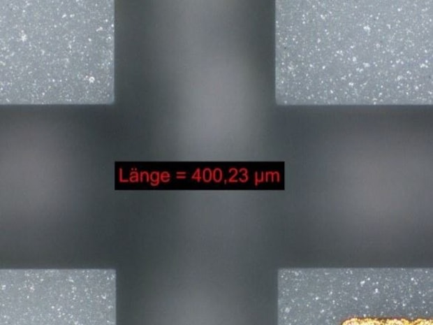
Application Examples for Dicing
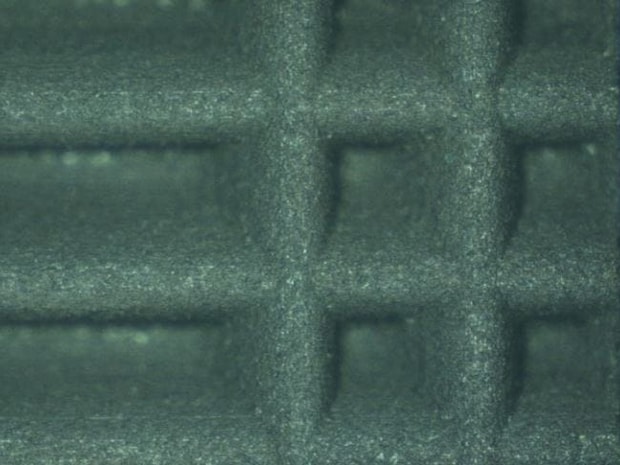
3D structure to increase adhesive surface (180µm)
Cut in sintered ceramics
Core competencies Die-Bonding
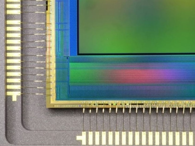
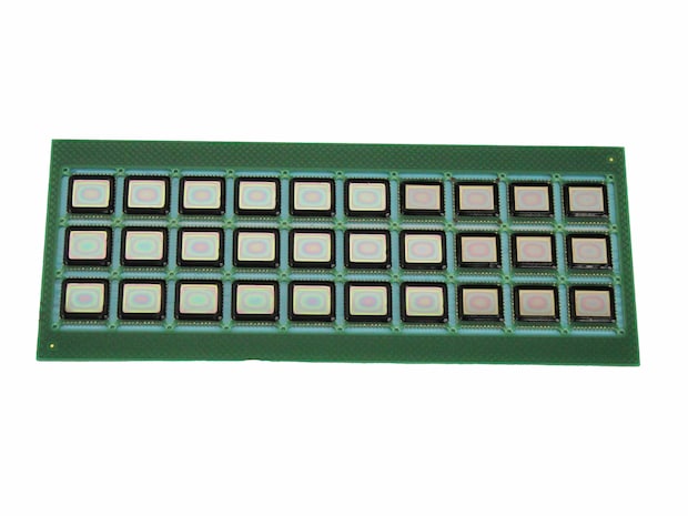
Full Format Image Sensor (Au, Ball-Wedge, 25µm)
Technology
- Adhesive die bonding (inline dispensing & stamping)
- Sintering
- Stacked die bonding
- Flip chip technology
Applications
- Wafer-level packaging (WLP) of MEMS and sensors
- Flip chip
- LED modules
- Image sensors
- Handling of image sensor with micro lens arrys
Substrates
- Circuit boards, wafers, component carriers, lead frames
Component dimensions
- 0.17mm up to 50mm
- > 25µm thickness
- Accuracy up to < 5µm
Component feed options:
- Wafer, waffle / Gel-Pak, reel
Marking
Technology
- Laser marking
- Printing system (Ink Jet)
Applications
- Traceability
Cleaning
Technology
- barrel reactor
Applications
- Clean organic residues from surface
- Activate surface (increase adhesion forces during joining processes)
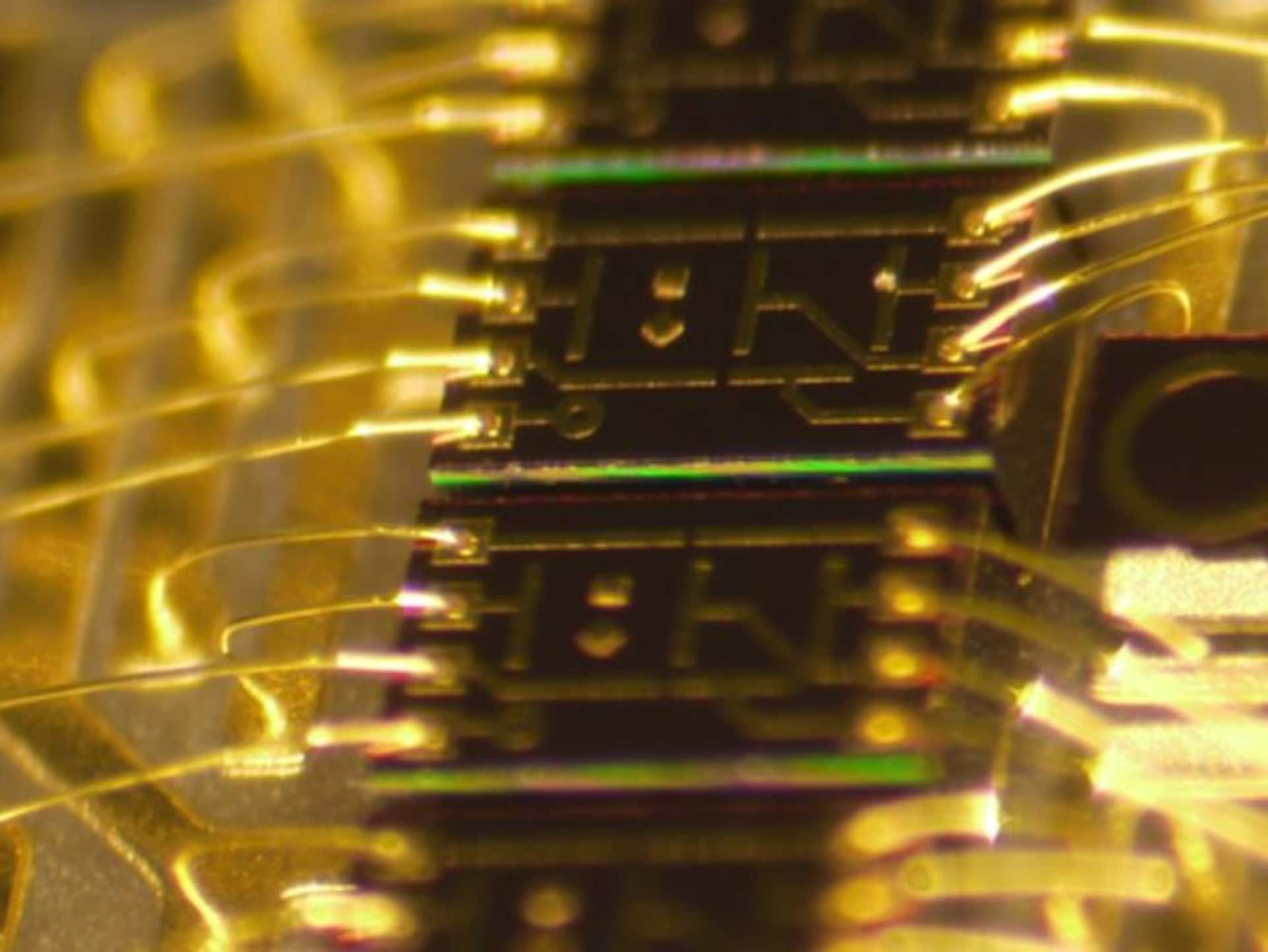
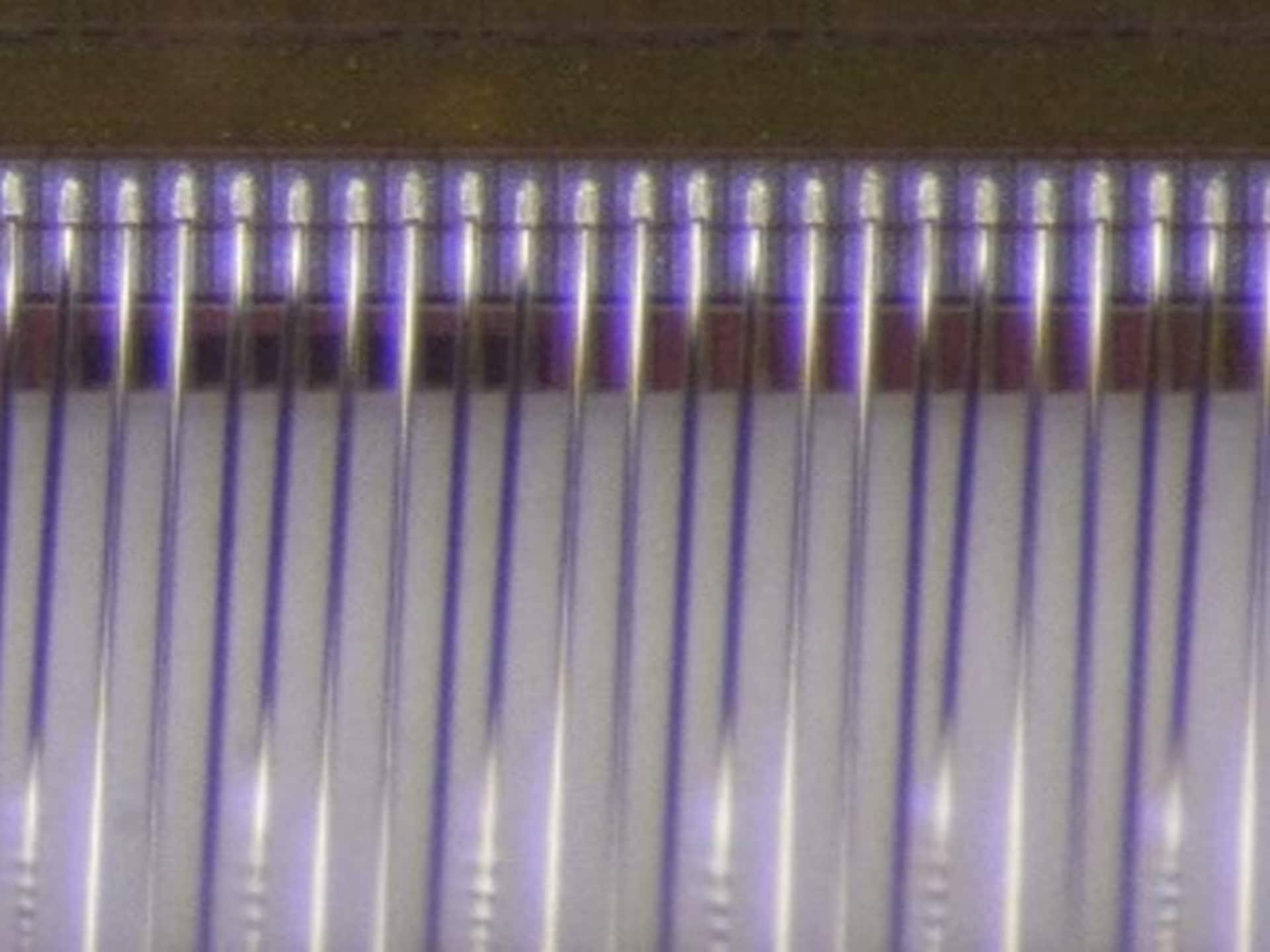
Core Competence Wire-bonding
Technology
- Wedge-Wedge and Ball-Wedge
- Accuracy bond tool: 2.5 µm
- Wire diameter: 12.5 µm up to 75 µm
- Material: gold, aluminum, silver, copper, and platinum
Core competence
- Adjust loop profile for ultra flat bonds
- Reflection-poor ball-wedge technology
Core competence Housing: Dispensing
Technology
- Accuracy 14µm
- Volume- or mass-controlled dispensing
- Volume accuracy: 0.1µl
Materials
- Silicone (in different cleanroom)
- 2/3K epoxy, polyurethane
Special competences
- Dam fill / underfill
- Black encapsulation to reduce reflections
- Mechanical protection
- Optical encapsulation to change light parameter
Core competence Housing: Set and seal optics
- Accuracy (regarding die-bonding) < 5µm
- Processing of special epoxy resins
- Minimization of trapped air (special evacuation procedure)
- Cavity flushing with N2 during the setting process
- Curing of potting with temperature or UV light
Core competence: EOL-Test
Opto-electrical measurement and AOI, contacting with card according to customer design
Probing-Station
- Accuracy up to 3µm
- Current-voltage characteristics
- 40W Current/voltage source with 4-point measurement
- Radiant intensity and wavelength measurement
- Automatic optical inspection (AOI)
- Applicatio12 MP Camera
- Switching/multiplexing with up to 32 contacts
- Logic measurements, multi-segment displays, etc.
- Flying probe
Further Product Recommendations

질문이 있으십니까? 저희 전문가들이 기꺼이 도와드립니다.


Digital Imaging & Optoelectronic Systems
HCI-CN-Carl-Wang
EditContact
+81 045 670-9141