RecommendMail Facebook LinkedIn
UFO Probe® 카드 - PIC 웨이퍼 테스트를 위한 새로운 테스트 카드
광집적 회로(PIC)는 미래의 칩입니다. 집적형 포토닉스는 데이터 및 신호 처리에 전기 대신 빛을 사용합니다.
The needs of chip manufacturers
- Increased chip complexity and integration density (SoC) through monolithic or heterogeneous integration of optics and electronics
- Economies of scale for cost optimization
- High-throughput test solutions for high-volume production
- High-yield mass production to reduce scrap and losses
- Automated test solutions
- Standardized tests
Challenges in Silicon Photonics Testing
- High-throughput test solutions (suitable for fab requirements) that perform electronic-photonics testing at the wafer level, with high parallelism and as much automation as possible
- Functional testing of PICs at an early stage in the process is critical for higher yields
- Standardization of the test environment and procedures is necessary to enable consistent and predictable testing of silicon photonics.
Free webinar recording: Watch it now and learn more!

“Just the Right PIC – How Advanced Test Concepts Enable Fast PIC Wafer-Level Testing!”
In this exclusive webinar recording, Tobias Gnausch (Jenoptik) and Sylwester Latkowski (TU Eindhoven) provide valuable insights into the following topics:
- Characterization vs. Testing: What are the differences, and why are both indispensable?
- Standardization as a foundation: How uniform test standards form the basis for high-volume production.
- Optoelectronic test methods: Practical approaches that allow you to significantly increase the efficiency of your wafer production
- Reliable testing without “active alignment”: Innovative techniques that eliminate the need for time-consuming alignments while guaranteeing the highest measurement accuracy.
세상을 더 빠르게 만듭니다
Custom-designed for a variety of applications
Unlike traditional test solutions, which use separate optical and electrical probe cards, Jenoptik combines an electrical and an optical test module into a single, compact test card. This test card is custom-designed and combines Jenoptik’s expertise in optics and photonics with the established probe technology of leading manufacturers.
Depending on your requirements, the UFO Probe® Card is configured and manufactured to meet your specific needs. Here are three examples of ProbeCard configurations we have already implemented. Contact us to discuss your individual requirements.

UFO Probe® Cantilever in Eurocard Format
- For vertically emitting PICs
- Monolithically integrated optical module with standardized or custom inputs and outputs
- Cantilever probe technology with several hundred probes
- Standard probe interface: Eurocard format
- Integrated distance sensor.

UFO Probe® Vertical in Eurocard format
General operating principle similar to that of the UFO Probe Cantilever, but particularly suitable for…
- High probe counts of up to tens of thousands of probes and beyond
- Extremely small probe sizes and spacings down to >40 µm
- Testing of pads and bumps
- Suitable for multi-DUT (multi-chip) and high-frequency (HF) testing.

UFO Probe® Vertical in ATE format
- Direct-docking design
- Interface for system integration into ATE (automated test equipment) platforms, such as Advantest V93000 or Teradyne UltraFlex
- For vertical-emitting PICs
- Ideal for a high number of electrical and optical contacts, as well as for multi-DUT testing.
Customized for your success
Each UFO Probe® Card is customized to the individual requirements and the respective wafer layout and is available with both cantilever and vertical needle technology. Check out the specifications for more details.

All benefits of the Probe Card Technology on one view
진행 과정
처리량이 많은 연속 생산에 적합한 효율적인 테스트 방법 덕분에 PIC 에코시스템을 확장할 수 있으며 여러 칩을 동시에 검증할 수 있어 테스트 시간을 단축할 수 있습니다.
혁신
표준 테스트 장비에서 실행할 수 있는 유일한 상용 대량 생산용 테스트 솔루션.
품질
생산 초기 단계에서 스크랩을 식별하여 수율을 높입니다: 모든 PIC의 각종 테스트를 웨이퍼에서 수행할 수 있습니다.
플러그 앤 플레이
표준 IC 테스터 및 자동 테스터에서 작동하도록 설계되었습니다. 낮은 지출 및 커미셔닝 비용.
효율성
불량 부품을 조기에 식별하여 수율을 높이고 생산 흐름을 최적화할 수 있습니다.
유연성
광학 I/O 채널의 피치 및 수를 사용자에 맞게 구성할 수 있습니다.
현재 및 향후 프로브 카드 적용 분야


UFO Probe® 카드를 사용하면 IC 및 PIC를 동시에 테스트할 수 있습니다
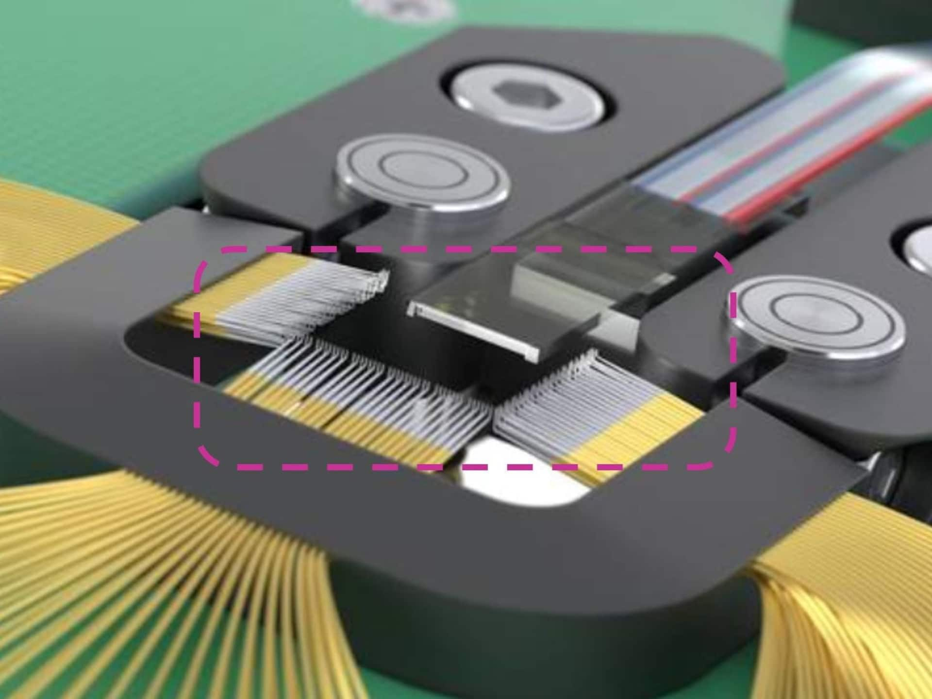
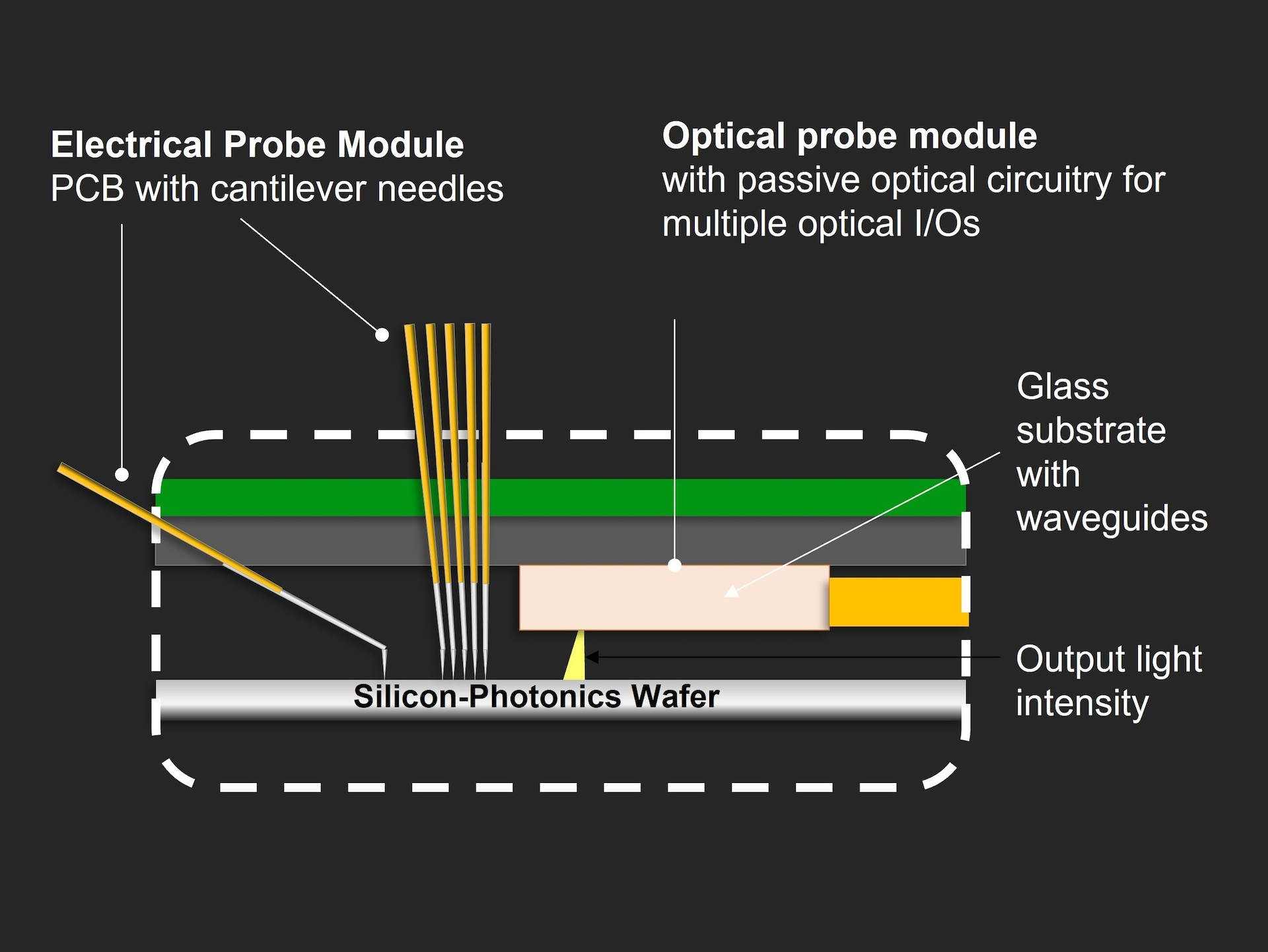
- Monolithically integrated optical module
- Alignment-insensitive optical coupling for vertically emitting PICs (compensates for probe tolerances)
- Simultaneous bonding of the chip’s optical and electrical interfaces
- Use of field-proven probe technologies
- Standard interfaces to testers and wafer probers
UFO Probe® 광전자 카드 기술 데이터
사양 | 현세대 | 미래 세대 |
테스트 대상 구성품 | 전자 및 광자 집적 회로(EPIC), 데이터 전송 및 통신 애플리케이션을 위한 광 트랜시버 | 트랜시버, 포토다이오드, |
전기 니들 기술 | 캔틸레버 | 캔틸레버,수직형/고급형 |
광학 커플링 원리 DUT | 수직 커플링 | 수직 커플링 |
광학 입력/출력(OI/OO) 개수 | 최대 16 | <200 |
피치 OI/OO | 250 μm | 유동적 |
OI/OO 어레이 레이아웃 구성 | 입력/출력 방향이 동일한 선형 배열 | 필요에 따라 구성 가능 |
커플링 브래킷 | 0° 및 11.6° | 0° - 20° |
지원되는 파장 | 1,310 nm 및 1,550 nm | VIS to NIR (U 대역) |
삽입 손실 측정 | 반복성: ~ 0.3 – 0.5 dB | 반복성 목표: 0.1 dB |
RF 측정 | 최대 100MHz | GHz |
인터페이스 | 유럽 카드 형식 | 유럽 카드 형식, |
Building on an existing and established IC testing ecosystem
Testing optical and electrical functionality is a critical factor in wafer manufacturing. Especially in high-volume production, it is essential to keep both test and setup times short while maintaining the highest possible yield to remain cost-effective. Here, the UFO Probe®Card offers a clever solution that leverages established IC test infrastructure developed over decades.Expand testing capacity or transition testing equipment to PIC


Your partner in PIC testing
Jenoptik has profound expertise and know-how in micro-optics and optics and we are a competent and valuable partner to the semiconductor industry for many years. We know and understand the challenges of our customers and combine these with our technical experience and knowledge to create innovative solutions, such as the UFO Probe®Card. The necessary skills and the continuous development of technologies is just one aspect that we pursue with one goal: Moving you forward.
High-Performance from A to Z – our competencies:
- Design: Optical module and general electrical and optical probe card card
- Manufacturing and supply chain management
- Micro-assembly and alignment of optical and electrical modules
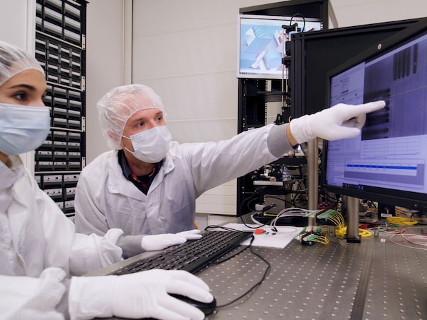
- Optical test and verification in lab: customized test rig
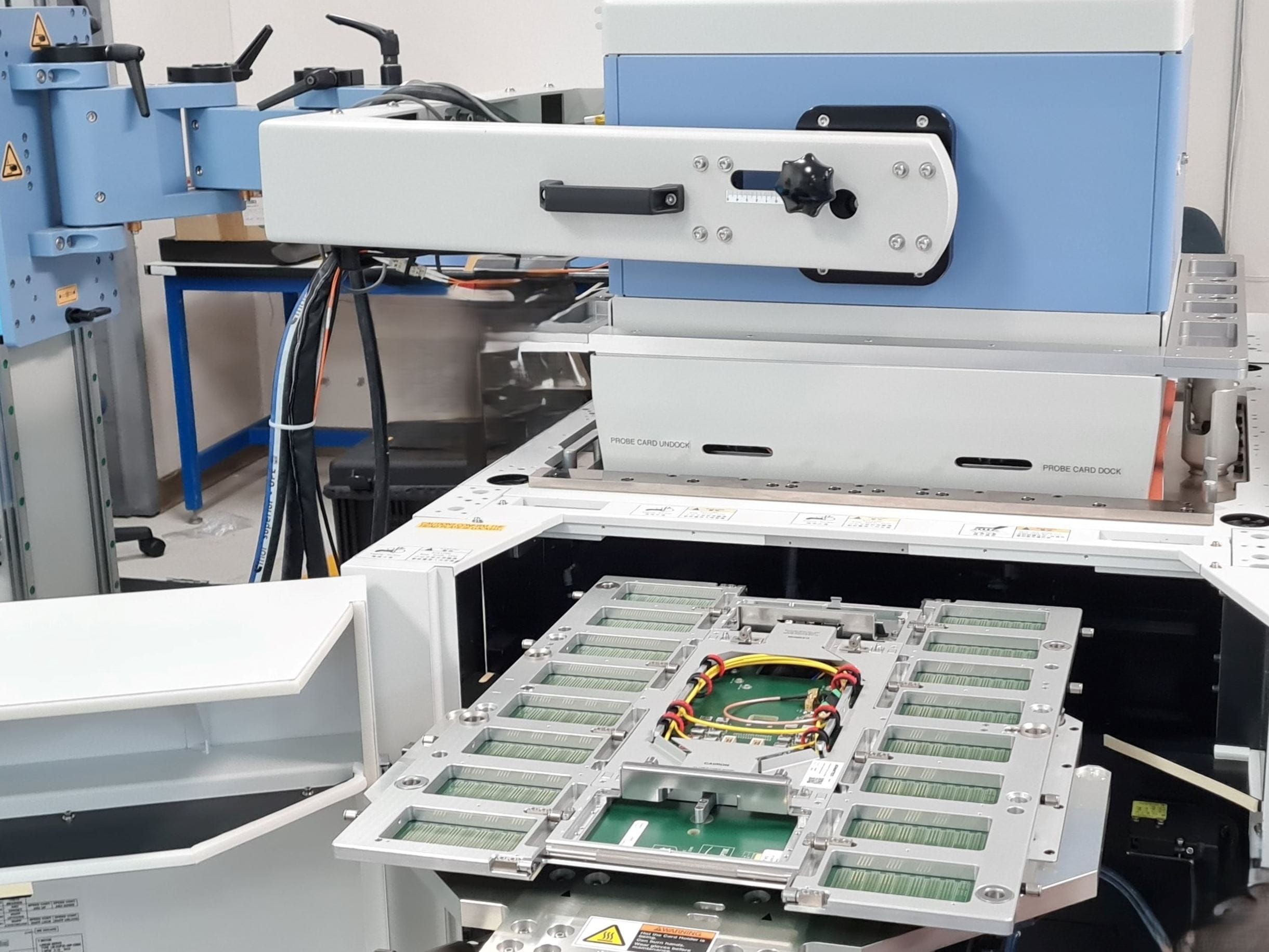
- Test under manufacturing conditions: Accretech UF3000 Prober

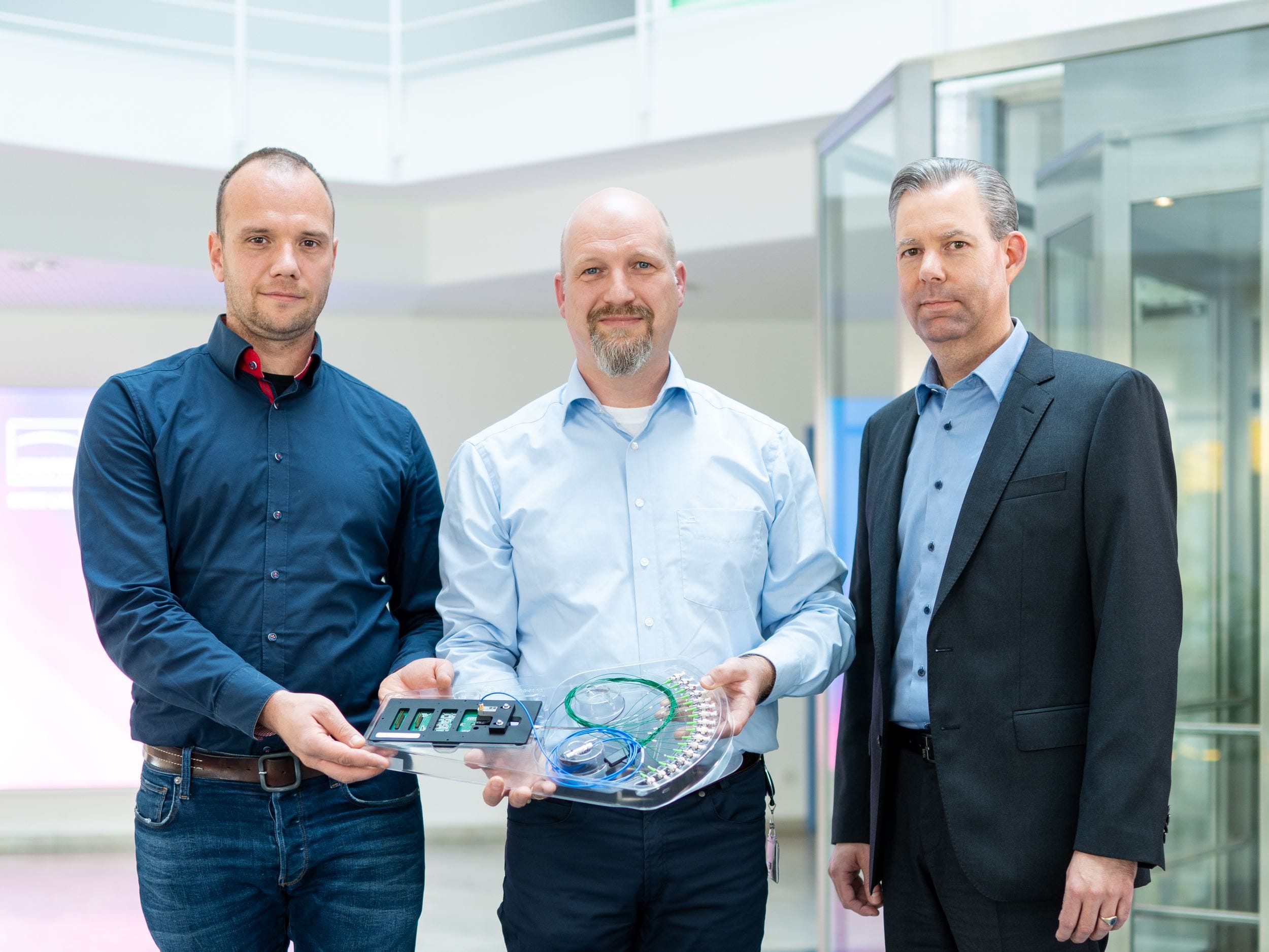
Awarded! Thuringia Innovation Award 2022 for UFO Probe® card
Jenoptik was awarded the Thuringia Innovation Award 2022 in the "Industry & Materials" category on November 30, 2022 in Weimar, Thuringia for its novel opto-electronic probe card for testing PIC wafers. Not quite 100 applications were received by STIFT Thüringen this year. Jenoptik convinced the expert jury with its well-thought-out approach to solving the increasing demand for photonic technologies in the electronics and semiconductor industry.